
Circuit Diagram
The circuit diagram of the single phase half wave controlled rectifier with resistive load is given in Fig. 1. The single phase half wave controlled rectifier circuit consists of a Thyristor switch only. An ac voltage source (vs) is connected at the input while a resistive (R) load is connected at the output. The thyristor is turned on after applying a firing pulse.
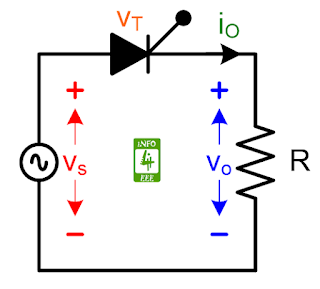 |
| Fig. 1 Circuit diagram of the single phase half wave controlled rectifier with resistive load. |
Working
The
single phase half wave controlled rectifier with resistive load operates in two modes.
Mode-1: Thyristor is OFF (0 to α and π to 2π)
During this mode, Thyristor is OFF. The equivalent circuit diagram of the single phase half wave controlled rectifier with the resistive load during mode-1 is given in Fig. 2. As the thyristor is OFF, hence output current will be zero. Therefore, the output voltage will also be zero. Hence all the input will be seen across the thyristor.
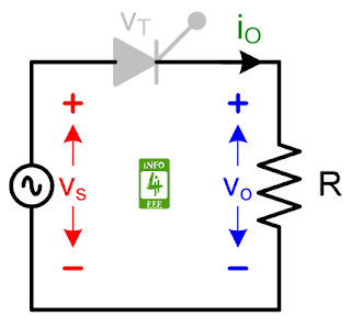 |
| Fig. 2 Equivalent circuit diagram of the single phase half wave controlled rectifier with the resistive load during Mode-1. |
Mode-2: Thyristor is ON (α to π)
During this mode, a firing pulse switched ON the Thyristor. The equivalent circuit diagram of the single phase half wave controlled rectifier with the resistive load during mode-2 is given in Fig. 3. As the Thyristor is ON, a small voltage will drop across the thyristor (let VT). While the voltage drop across the thyristor is considered zero in this article. Hence all the input will be seen across the output.
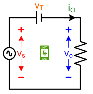 |
| Fig. 3 Equivalent circuit diagram of the single phase half wave controlled rectifier with the resistive load during Mode-2. |
The average value of output voltage across the resistor (R) is calculated with the following expression.
The maximum value of output voltage across the resistor (R) is calculated with the following expression.
The normalized value of output voltage across the resistor (R) is calculated with the following expression.
Vn = Vdc/Vdcm = 0.5 (1+cosα)
The rms value of output voltage across the resistor (R) is calculated with the following expression.
Vrms = (Vm/2) ✕ [(1/π) ( π - α + (sin2α)/2 )]^(1/2)
Waveforms
The waveforms for the single phase half wave controlled rectifier with resistive load are shown in Fig. 4. The waveform of the ac input voltage source is shown in red color. The waveform of the firing signal is shown with pink color. The waveform of the voltage across the resistive load is shown with blue color. The waveform of the current through the resistive load is shown with green color. The waveform of the voltage across the thyristor is shown with orange color.
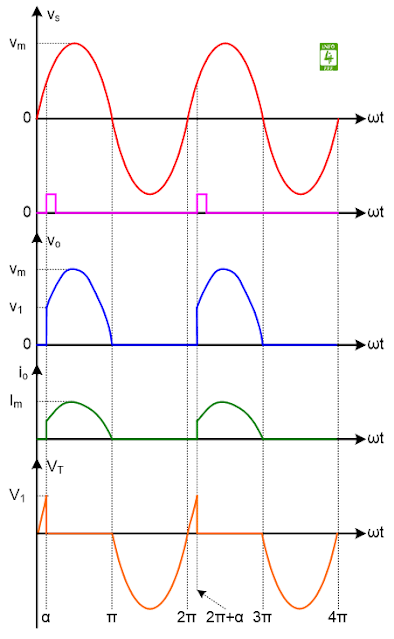 |
| Fig. 4 Waveforms for the single phase half wave controlled rectifier with resistive load. |
Reference
M. H. Rashid, “Power Electronics: Circuits, Devices, and Applications,” Prentice Hall India, Second Edition, pp. 131-132, 2006.
Author


Post a Comment