
Circuit Diagram
The circuit diagram of the step-up chopper with resistive load is given in Fig. 1. The step-up chopper consists of an IGBT switch (S), an inductor (L), and a diode (D). A dc voltage source (VS) is connected at the input while a resistive load (R) is connected at the output. The switch (S) is operated with the switching signal of 50 % duty cycle.
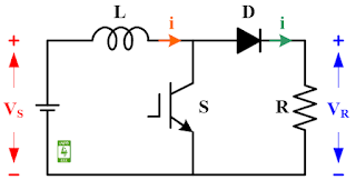 |
Fig. 1 Circuit diagram of the step-up chopper with resistive load.
|
Working
The step-up chopper with resistive load operates in two modes.
Mode-1: Switch (S) is ON
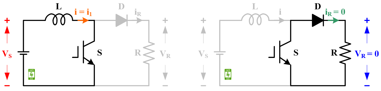
During this mode, high switching the signal (S = 1) is fed to the gate terminal to turn ON the IGBT switch. The equivalent circuit diagram of the step-up chopper with resistive load during mode-1 is given in Fig. 2. During this mode, The circuit diagram of the step-up chopper with the resistive load is split in to two separate loops. First loop consists of dc voltage source, inductor, and switch. As switch is ON, small voltage will drop across the switch (let VSW) and rest of the voltage (VS-VSW) charge the inductor with the current (i1). Second loop consists of swtich, diode, and resistor. As there is no voltage source in the loop, the current through the resistive load and voltage across the resistive load will be zero.
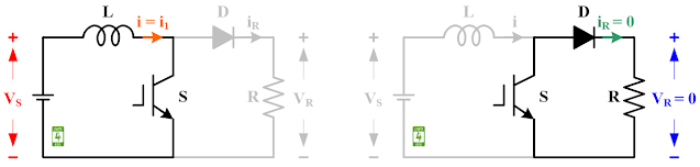 |
| Fig. 2 Equivalent circuit diagram of the step-up chopper with the resistive load during Mode-1. |
The current across the inductor (L) is calculated with the following equation.
VS = L di1/dt
While peak-to-peak ripple current in the inductor is calculated with the following equation.
ΔI = VS/L 🗙 t1
The instantaneous value of current (i1) is calculated with the following equation.
i1 = VS/L 🗙 t + I1
Mode-2: Switch (S) is OFF
During this mode, a low switching signal (S = 0) is fed to the gate terminal to turn OFF the IGBT switch. The equivalent circuit diagram of the step-up chopper with the resistive load during mode-2 is given in Fig. 3. During this mode, the circuit diagram of the step-up chopper with resistive load makes a loop that consists of the dc voltage source, inductor, diode, and resistive load. The voltage of the dc source (VS) along with voltage across the inductor (VL) is seen across the load. As the inductor is connected to the resistive load, the inductor discharge through the resistive load with the current (i2). The diode prevents the reverse flow of current.
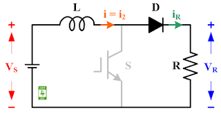 |
| Fig. 3 Equivalent circuit diagram of the step-up chopper with the resistive load during Mode-2. |
The instantaneous value of output voltage across the resistor (R) is calculated with the following expression.
The instantaneous value of output voltage across the resistor (R) in terms of duty cycle is calculated with the following expression.
vO = VS/(1-k)
Waveforms
The waveforms for the step-up chopper with resistive load are shown in Fig. 4. The waveform of the switching signal of the 50 % duty cycle is shown in pink color. The waveform of the constant voltage source is shown in red color. The waveform of the voltage across the resistive load is shown in blue color. The waveform of the current through the resistive load is shown in green color. The waveform of the current through the inductor is shown in orange color.
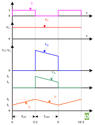 |
| Fig. 4 Waveforms for the step-up chopper with resistive load. |
Reference
M. H. Rashid, “Power Electronics: Circuits, Devices, and Applications,” Prentice Hall India, Second Edition, pp. 309-312, 2006.
Author


Post a Comment