Transistor and it's practical applications
What is Transistor :- Transistor is a three layer, three terminal,two junction, non linear semiconductor solid state device. Transistor is a combination of transfer and resistor which means Transistor mainly does transfer of resistance. Transistor is used for switching, amplification, oscillations generation and buffering etc. Transistor is made either by sandwiching one P type layer in between two N type layers or by sandwiching one N type layer in between two P type layer. Three terminals of Transistor are called emitter, base and collector.
Important point:- Emitter is highly doped, base is lightly doped and collector is moderately doped.
Regions of Transistor working:-
1. Active region:- Active region is mainly used for amplification purpose in which first junction(Emitter base junction) is kept forward biased and second junction (Collector base junction) is kept reverse biased.
2. Saturation region:- In this mode both of the junction are kept forward biased.
3. Cut off region:- In this mode both of the junction are kept reverse biased. Saturation and cut off modes are combinely used in switching devices.
4. Inverted region:- In this mode first junction (Emitterbasejunction) is kept reverse biased and second junction (Collectorbasejunction) is kept forward biased. This mode is just reverse to active mode.
Transistor can be connected in a circuit in three configurations:-
1. Common Base Configuration
2. Common Emitter configuration
3. Common Collector Configuration
Common emitter configuration is highly used beacuse of medium to high voltage gain, high power gain, high current gain, and better performance.
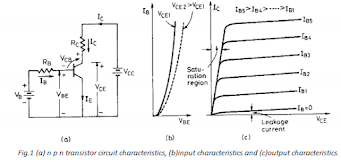
Fig 1(a) shows connection diagram of CE configuration where
IB = (VB - VBE) / RB
IC = βDC×IB
VCC = RC × IC + VCE
Where βDC is current gain.
Characteristics is mainly Voltage and current curve which shows behaviour of Transistor in working condition. In input characteristics graph is made between input voltage (VBE) and input current (IB) where as output characteristics is graph between output voltage (VCE ) and output current (IC).
When two points saturation point and cut off point on the output characteristics are joined by a straight line we get a DC load line. It is called a DC load line because its slope depends upon the load resistance RC which is a DC load. The point where DC load line intersects output characteristics of transistor is called Quiescent point. The concept of Q point is used when transistor is used as an amplifier i.e. operate in active region of output characteristics.
Important points :-
1. Base bias is a prototype used in the design of switching circuits.
2. Emitter bias is a prototype used in the design of amplifying circuits.
3. Most widely used biasing circuit is voltage divider beacuse this biasing is more stable and less temperature dependent.
4. Some power transistors have only two leads and their body acts as collector terminal.
Author:- Amarjeet Singh Jamwal authored articles on Basic Electronics Engineering, Electric Traction, and Electronics Practical for INFO4EEE Website

.jpeg)


Post a Comment