
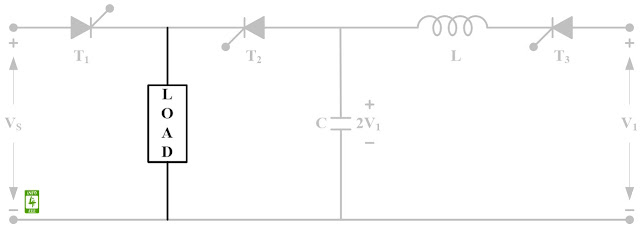
External Pulse Commutation of Thyristor

External pulse commutation is also called Class-E commutation. A circuit diagram of the external pulse commutation of the thyristor is given in Fig. 1.
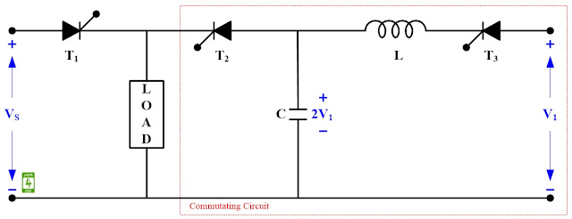 |
| Fig. 1 Circuit diagram of external pulse commutation. |
A pulse of voltage is obtained from a separate voltage source to turn OFF the conducting thyristor. Auxiliary source voltage (V1) is greater than the source voltage (VS). When the T1 is conducting, the source is connected to the load as given in Fig. 2.
Case-1: At t = 0, T3 is turned ON. V1, T3, L, and C form an oscillatory circuit. Therefore, C is charged to a voltage +2V1 at t = π✓LC as given in Fig. 2.
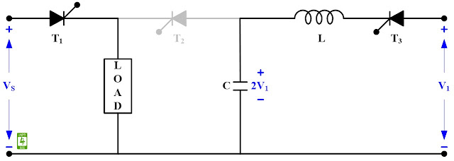 |
| Fig. 2 Equivalent circuit when source is connected to load. |
As oscillatory current falls to zero, T3 gets commutated and equivalent circuit is given in Fig. 3.
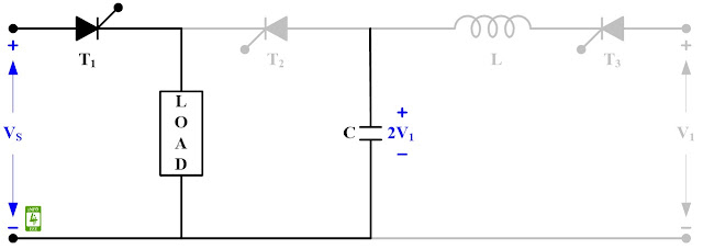 |
| Fig. 3 Equivalent circuit after the commutation of T3. |
Case-2: For turning OFF T1, T2 is turned ON. Now (VS-2V1) is applied across T1 and T1 is turned OFF as given in Fig. 4.
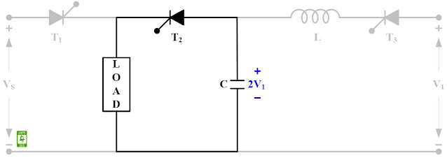 |
| Fig. 4 Equivalent circuit after the commutation of T1. |
After this, the capacitor discharges through the load and equivalent circuit is given in Fig. 5.
 |
| Fig. 5 Equivalent circuit after discharging of capacitor. |
Reference
Author


Post a Comment